- 您现在的位置:买卖IC网 > Sheet目录3862 > PIC18F45J11-I/ML (Microchip Technology)IC PIC MCU FLASH 32K 2V 44-QFN
2010 Microchip Technology Inc.
DS70138G-page 131
dsPIC30F3014/4013
19.0
12-BIT ANALOG-TO-DIGITAL
CONVERTER (ADC) MODULE
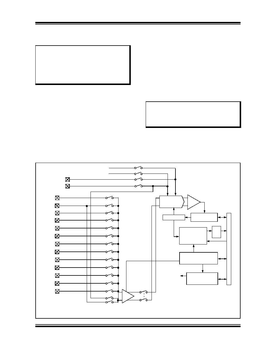
The 12-bit Analog-to-Digital Converter (ADC) allows
conversion of an analog input signal to a 12-bit digital
number. This module is based on a Successive
Approximation Register (SAR) architecture and pro-
vides a maximum sampling rate of 200 ksps. The A/D
module has up to 16 analog inputs which are multi-
plexed into a sample and hold amplifier. The output of
the sample and hold is the input into the converter
which generates the result. The analog reference volt-
age is software selectable to either the device supply
voltage (AVDD/AVSS) or the voltage level on the
(VREF+/VREF-) pin. The A/D converter has a unique
feature of being able to operate while the device is in
Sleep mode with RC oscillator selection.
The A/D module has six 16-bit registers:
A/D Control Register 1 (ADCON1)
A/D Control Register 2 (ADCON2)
A/D Control Register 3 (ADCON3)
A/D Input Select Register (ADCHS)
A/D Port Configuration Register (ADPCFG)
A/D Input Scan Selection Register (ADCSSL)
The ADCON1, ADCON2 and ADCON3 registers
control the operation of the A/D module. The ADCHS
register selects the input channels to be converted. The
ADPCFG register configures the port pins as analog
inputs or as digital I/O. The ADCSSL register selects
inputs for scanning.
The block diagram of the 12-bit A/D module is shown in
FIGURE 19-1:
12-BIT A/D FUNCTIONAL BLOCK DIAGRAM
Note:
This data sheet summarizes features of
this group of dsPIC30F devices and is not
intended to be a complete reference
source. For more information on the CPU,
peripherals,
register
descriptions
and
general device functionality, refer to the
“dsPIC30F Family Reference Manual”
(DS70046).
Note:
The SSRC<2:0>, ASAM, SMPI<3:0>,
BUFM and ALTS bits, as well as the
ADCON3 and ADCSSL registers, must
not be written to while ADON = 1. This
would lead to indeterminate results.
Comparator
12-Bit SAR
Conversion Logic
VREF+
DAC
Da
ta
16-Word, 12-Bit
Dual Port
RAM
B
u
s
I
n
te
rf
ac
e
AN12
0000
0101
0111
1001
1100
0001
0010
0011
0100
0110
1000
1010
1011
AN8
AN9
AN10
AN11
AN4
AN5
AN6
AN7
AN0
AN1
AN2
AN3
CH0
AN1
VREF-
Sample/Sequence
Control
Sample
Input MUX
Control
Input
Switches
S/H
AVSS
AVDD
Fo
rm
a
t
Note:
The ADCHS, ADPCFG and ADCSSL registers allow the application to configure AN13-AN15 as analog input
pins. Since these pins are not physically present on the device, conversion results from these pins will read ‘0’.
发布紧急采购,3分钟左右您将得到回复。
相关PDF资料
SFW15R-2STE1
SFW15R-2STE1-FFC/FPC CONN
PIC18F26J11-I/ML
IC PIC MCU FLASH 64K 2V 28-QFN
PIC18F46K20-E/ML
IC PIC MCU FLASH 32KX16 44QFN
PIC24FJ64GA002-I/SO
IC PIC MCU FLASH 64KB 28SOIC
PIC16C711-04/P
IC MCU OTP 1KX14 A/D 18DIP
PIC18LF26K22-I/SP
IC PIC MCU 64KB FLASH 28SPDIP
PIC18F25K80-I/SP
MCU PIC 32KB FLASH 28SDIP
DSPIC33FJ12MC201-I/SS
IC DSPIC MCU/DSP 12K 20SSOP
相关代理商/技术参数
PIC18F45J11-I/PT
功能描述:8位微控制器 -MCU 32KB Flash 4KBRAM 12MIPS nanoWatt RoHS:否 制造商:Silicon Labs 核心:8051 处理器系列:C8051F39x 数据总线宽度:8 bit 最大时钟频率:50 MHz 程序存储器大小:16 KB 数据 RAM 大小:1 KB 片上 ADC:Yes 工作电源电压:1.8 V to 3.6 V 工作温度范围:- 40 C to + 105 C 封装 / 箱体:QFN-20 安装风格:SMD/SMT
PIC18F45J11T-I/ML
功能描述:8位微控制器 -MCU 32KB Flash 4KBRAM 12MIPS nanoWatt RoHS:否 制造商:Silicon Labs 核心:8051 处理器系列:C8051F39x 数据总线宽度:8 bit 最大时钟频率:50 MHz 程序存储器大小:16 KB 数据 RAM 大小:1 KB 片上 ADC:Yes 工作电源电压:1.8 V to 3.6 V 工作温度范围:- 40 C to + 105 C 封装 / 箱体:QFN-20 安装风格:SMD/SMT
PIC18F45J11T-I/PT
功能描述:8位微控制器 -MCU 32KB Flash 4KBRAM 12MIPS nanoWatt RoHS:否 制造商:Silicon Labs 核心:8051 处理器系列:C8051F39x 数据总线宽度:8 bit 最大时钟频率:50 MHz 程序存储器大小:16 KB 数据 RAM 大小:1 KB 片上 ADC:Yes 工作电源电压:1.8 V to 3.6 V 工作温度范围:- 40 C to + 105 C 封装 / 箱体:QFN-20 安装风格:SMD/SMT
PIC18F45J50-I/ML
功能描述:8位微控制器 -MCU Full Spd USB 32KB 4KBRAM nanoWatt RoHS:否 制造商:Silicon Labs 核心:8051 处理器系列:C8051F39x 数据总线宽度:8 bit 最大时钟频率:50 MHz 程序存储器大小:16 KB 数据 RAM 大小:1 KB 片上 ADC:Yes 工作电源电压:1.8 V to 3.6 V 工作温度范围:- 40 C to + 105 C 封装 / 箱体:QFN-20 安装风格:SMD/SMT
PIC18F45J50-I/PT
功能描述:8位微控制器 -MCU Full Spd USB 32KB 4KBRAM nanoWatt
RoHS:否 制造商:Silicon Labs 核心:8051 处理器系列:C8051F39x 数据总线宽度:8 bit 最大时钟频率:50 MHz 程序存储器大小:16 KB 数据 RAM 大小:1 KB 片上 ADC:Yes 工作电源电压:1.8 V to 3.6 V 工作温度范围:- 40 C to + 105 C 封装 / 箱体:QFN-20 安装风格:SMD/SMT
PIC18F45J50T-I/ML
功能描述:8位微控制器 -MCU Full Spd USB 32KB 4KBRAM nanoWatt RoHS:否 制造商:Silicon Labs 核心:8051 处理器系列:C8051F39x 数据总线宽度:8 bit 最大时钟频率:50 MHz 程序存储器大小:16 KB 数据 RAM 大小:1 KB 片上 ADC:Yes 工作电源电压:1.8 V to 3.6 V 工作温度范围:- 40 C to + 105 C 封装 / 箱体:QFN-20 安装风格:SMD/SMT
PIC18F45J50T-I/PT
功能描述:8位微控制器 -MCU Full Spd USB 32KB 4KBRAM nanoWatt RoHS:否 制造商:Silicon Labs 核心:8051 处理器系列:C8051F39x 数据总线宽度:8 bit 最大时钟频率:50 MHz 程序存储器大小:16 KB 数据 RAM 大小:1 KB 片上 ADC:Yes 工作电源电压:1.8 V to 3.6 V 工作温度范围:- 40 C to + 105 C 封装 / 箱体:QFN-20 安装风格:SMD/SMT
PIC18F45K20-E/ML
功能描述:8位微控制器 -MCU 32KB Flash 1536B RAM 25 I/O 8B RoHS:否 制造商:Silicon Labs 核心:8051 处理器系列:C8051F39x 数据总线宽度:8 bit 最大时钟频率:50 MHz 程序存储器大小:16 KB 数据 RAM 大小:1 KB 片上 ADC:Yes 工作电源电压:1.8 V to 3.6 V 工作温度范围:- 40 C to + 105 C 封装 / 箱体:QFN-20 安装风格:SMD/SMT